
International GaN Workshop at Schloss Ringberg
January 20 - 24 1998
Surface Morphology, Interfaces and Growth of the III-Nitrides
Organized By:J. Neugebauer1, M. Scheffler1 and B. Meyer2
1
Fritz-Haber-Institut der Max-Plack-Gesellschaft2
University of GiessenList of Contents:
Despite progress in fabricating GaN based devices, achieving insight into the fundamental growth mechanisms of GaN is still in its infancy. Even basic properties of surfaces, surface diffusion, and interfaces such as stoichiometry, atomic geometry, and band structure are not well understood. A deeper knowledge of these mechanisms is crucial to improve growth in a systematic way, thereby enabling low background carrier concentrations and dislocation densities to be obtained.
The objective of this international workshop is to provide a forum for nitride researchers to exchange their knowledge by presenting their latest results. The workshop is limited to 60 participants enabling in-depth technical discussions. The focus will be on latest experimental and theoretical results concerning the properties of surfaces, internal and external interfaces, and growth with particular emphasize on atomic scale processes.
The workshop will begin on Tuesday, January 22 at 6 p.m. and will end on Saturday after breakfast.
Topics:
|
Surfaces: |
|
|
F. Bechstedt (Jena, Germany) |
Chemical Trends in Surface Properties of III-Nitrides |
|
J. Bernholc (Raleigh, USA) |
Theory of Surfaces, Adsorbates, Heterostructures, Defects and Ordering in Nitride Semiconductors |
|
O. Brandt (Berlin, Germany) |
Surfaces and Interfaces in the GaN/GaAs Materials System |
|
G. Feuillet (Grenoble, France) |
Surface Reconstructions and 2D/3D Growth Processes for Nitride Semiconductors |
|
J. E. Northrup (Palo Alto, USA) |
Structure, Energetics, and Electronic Properties of GaN and AlN Surfaces |
|
A.R. Smith (Pittsburgh, USA) |
Surface Reconstructions of Wurtzite GaN Studied by Scanning Tunneling Microscopy |
|
T. Zywietz (Berlin, Germany) |
Surfaces, Surfactants, and Diffusion at Cubic and Hexagonal GaN |
|
Interfaces: |
|
|
V. Fiorentini (Cagliari, Italy) |
Polarization, Offsets, and Device Design of III-N Nanostructures |
|
H. Lüth (Jülich, Germany) |
Valence Band Offsets at SiC/AlN/GaN Heterojunctions |
|
W. Mönch (Duisburg, Germany) |
Electronic Properties of Metals on Group-III Nitrides: Three Examples |
|
P. Vogl (München, Germany) |
Energetics and Atomic Structure of the SiC/GaN, SiC/AlN Interfaces |
|
C. G. Van de Walle (Palo Alto, USA) |
Interfaces and Band Offsets in III-Nitrides |
|
Growth: |
|
|
H. Amano (Tokyo, Japan) |
In situ Observation of the Crystallization Process of the Low Temperature Deposited Buffer Layer on Sapphire |
|
T. Fraunheim (Chemnitz, Germany) |
Ab initio Selfconsistent-Charge Tight-Binding: Applications to III-V Semiconductor Surfaces and Dislocations |
|
D. Hommel (Bremen, Germany) |
Comparison of Structural and Electrical Properties of GaN Layers Grown with ECR- and rf-Plasma Sources |
|
M. Kamp (Ulm, Germany) |
Growth Kinetics of Group III-Nitrides Using Ammonia in MBE |
|
H. Lakner (Duisburg, Germany) |
Nanostructure and Spatially Resolved Electro-Optical Properties of Group III-Nitride Quantum Wells |
|
B. Meyer (Giessen, Germany) |
Low Presure CVD Growth of GaN - Structural, Optical and Electrical Properties |
|
H. Riechert (München, Germany) |
MBE Growth of GaN |
|
J. Speck (Santa Barbara, USA) |
Defect Generation and Morphological Evolution in GaN Heteroepitaxy |
|
O. Ambacher (München, Germany) |
Consequences of the Special Physical and Chemical Properties on the Growth of Group-III Nitride Heterostructures by MBE and MOCVD |
|
H. Obloh (Freiburg, Germany) |
Issues of Growth, Morphology and Interface-Abruptness of III-Nitride Heterostructures Grown by MOCVD |
|
T. Suski (Warsaw, Poland) |
Role of High Pressure in GaN Crystal Growth, Activation of Impurities and Defect Annihilation |
|
E. Weber (Berkeley, USA) |
Thin film Growth of GaN: The Role of Strain, Stoichiometry and Doping |
Tuesday, Jan. 20 (Opening)
|
15:00 - 18:00 |
Registration |
|
|
18:30 - 20:00 |
Dinner |
|
|
20:00 - 20:15 |
Opening (J. Neugebauer, B. Meyer, M. Scheffler) |
|
|
Chair: J. Pollmann |
||
|
20:15 - 21:00 |
A.R. Smith (Pittsburgh, USA) |
Surface reconstructions of wurtzite GaN studied by scanning tunneling microscopy |
|
21:00 - 21:45 |
J. E. Northrup (Palo Alto, USA) |
Structure, energetics, and electronic properties of GaN and AlN surfaces |
|
21:45 |
Welcome Party (sponsored by AIXTRON AG) |
|
Wednesday, Jan. 21 (Surfaces)
|
8:00 - 9:00 |
Breakfast |
|
|
Chair: P. Boguslawski |
||
|
9:00 - 9:45 |
G. Feuillet (Grenoble, France) |
Surface reconstructions and 2D/3D growth processes for nitride semiconductors |
|
9:45 - 10:30 |
T. Zywietz (Berlin) |
Surfaces, Surfactants and Diffusion at Cubic and Hexagonal GaN |
|
10:30 - 11:00 |
Coffee break |
|
|
Chair: M. Scheffler |
||
|
11:00 - 11:45 |
F. Bechstedt (Jena) |
Chemical trends in surface properties of III-nitrides |
|
11:45 - 12:30 |
J. Bernholc (Raleigh, USA) |
Theory of Surfaces, Adsorbates, Heterostructures, Defects and Ordering in Nitride Semiconductors |
|
12:30 |
Lunch |
|
|
14:00 |
Guided tour through the castle |
|
|
15:00 - 17:00 |
Poster Session I |
|
|
Chair: D. Bimberg |
||
|
17:00 - 17:45 |
O. Brandt (Berlin) |
Surfaces and interfaces in the GaN/GaAs materials system |
|
17:45 - 18:30 |
H. Lüth (Juelich) |
Valence Band Offsets at SiC/AlN/GaN Heterojunctions |
|
18:30 - 20:00 |
Dinner |
|
|
20:00 - |
Rump Session (J. Neugebauer) |
Properties and morphology of surfaces and interfaces |
Thursday, Jan. 22 (Interfaces)
|
8:00 - 9:00 |
Breakfast |
||
|
Chair: K. Horn |
|||
|
9:00 - 9:45 |
H. Lakner (Duisburg) |
Nanostructure and spatially resolved electro-optical properties of group III-nitride quantum wells |
|
|
9:45 - 10:30 |
T. Fraunheim (Chemnitz) |
Ab initio selfconsistent-charge tight-binding: applications to III-V semiconductor surfaces and interfaces |
|
|
10:30 - 11:00 |
Coffee break |
||
|
Chair: A. Rizzi |
|||
|
11:00 - 11:45 |
W. Mönch (Duisburg) |
Electronic properties of metals on group-III nitrides: Three examples |
|
|
11:45 - 12:30 |
C. G. Van de Walle (Palo Alto, USA) |
Interfaces and band offsets in III-nitrides |
|
|
12:30 |
Lunch |
||
|
14:00 |
Walk through the winter forest |
|
|
|
16:00 - 17:00 |
Poster Session II |
|
|
|
Chair: R. Nieminen |
|||
|
17:00 - 17:45 |
V. Fiorentini (Cagliari, Italy) |
Polarization, Offsets, and Device Design of III-N Nanostructures |
|
|
17:45 - 18:30 |
P. Vogl (München) |
Energetics and Atomic Structure of the SiC/GaN, SiC/AlN Interfaces |
|
|
18:30 - 20:00 |
Dinner |
||
|
20:00 - |
Concert |
||
Friday, Jan. 23 (Growth)
|
8:00 - 9:00 |
Breakfast |
|
|
Chair: J. Neugebauer |
||
|
9:00 - 9:45 |
H. Amano (Nagoya, Japan) |
In situ observation of the crystallization process of the low temperature deposited buffer layer on sapphire |
|
9:45 - 10:30 |
D. Hommel (Bremen) |
Comparison of structural and electrical properties of GaN layers grown with ECR- and rf-plasma sources |
|
10:30 - 11:00 |
Coffee break |
|
|
Chair: A. Krost |
||
|
11:00 - 11:45 |
J. Speck (Santa Barbara, USA) |
Defect generation and morphological evolution in GaN heteroepitaxy |
|
11:45 - 12:30 |
B. Meyer (Giessen) |
Low pressure CVD growth of GaN - structural, optical and electrical properties |
|
12:30 |
Lunch |
|
|
Chair: J. Christen |
||
|
14:15 - 15:00 |
H. Obloh |
Issues of growth, morphology and interface-abruptness of III-Nitride heterostructures grown by MOCVD |
|
15:00 - 15:45 |
H. Riechert (München) |
MBE Growth of GaN |
|
Chair: D. As |
||
|
15:45 - 16:30 |
T. Suski (Warsaw, Poland) |
Role of high pressure in GaN crystal growth, activation of impurities and defect annihilation |
|
16:30 - 17:00 |
Coffee break |
|
|
Chair: B. Meyer |
||
|
17:00 - 17:45 |
O. Ambacher (München) |
Consequences of the special physical and chemical properties on the growth of group-III nitride heterostructures by MBE and MOCVD |
|
17:45 - 18:30 |
M. Kamp (Ulm) |
Growth kinetics of group III nitrides using ammonia in MBE |
|
18:30 - 20:00 |
Dinner |
|
|
20:00 - 20:45 |
E. Weber (Berkeley, USA) |
Thin film growth of GaN: the role of strain, stoichiometry and doping |
|
20:45 - |
Rump Session (M. Kamp, H. Riechert, J. Speck) |
Growth Techniques and Mechanisms |
Saturday, Jan. 24 (Departure)
|
8:00 - 9:00 |
Breakfast |
|
|
9:00 |
Check Out and Departure |
|
4. Information about Schloss Ringberg
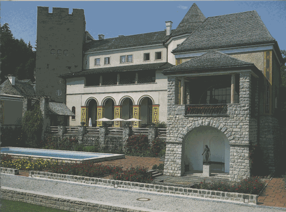
Schloss Ringberg
D-83700 Rottach-Egern
Germany
The weather in January is typically quite cold (average between -5 and 5
° C, 55 - 65 F) with occasional snowfall. Be prepared for winter like weather.5. Submission of Abstracts
Abstract Deadline: October 31, 1997
Please send the abstracts to the following address:
Registration Deadline: November 30, 1997
There will be no registration fee. The cost for full board and lodging will be 500 DM.
This includes the room rate for four nights, breakfast, lunch and dinner. Please note that we cannot accept credit cards! On Tuesday, January 20, there will be dinner only. On Saturday, January 24, breakfast will be served.To register, please send an e-mail with your name, affiliation and arrival time to:
For young scientists presenting a contributed talk or poster there may be financial support covering the costs for full board and lodging.
The workshop will be sponsored by the Deutsche Forschungsgemeinschaft (DFG) and the Max-Plack-Gesellschaft (MPG). The social program will be sponsored by the AIXTRON AG (
http://www.aixtron.com/).
![]()

This Page is maintained by: Tosja Zywietz
Last update: January 13, 1998