
Workshop at Schloss Ringberg, Rottach-Egern, Germany
7.- 10. February 2001
Growth, electronic and optical properties of low-dimensional semiconductor quantum structures
organized by:P. Kratzer1, K. Jacobi1 and M. Scheffler1
1
Fritz-Haber-Institut der Max-Plack-GesellschaftList of Contents:
This workshop is intended as an informal discussion meeting to bring together leading scientists who are interested in experiments on growth and characterization of semiconductor quantum structures, in applications of these nanostructures and in the theory of semiconductor growth.
Topics:
A very important and active field in semiconductor solid state physics is the fabrication of low-dimensional structures which allow the confinement of charge carriers in dimensions near to their de-Broglie-wavelength. Such systems allow an engineering of the electronic and vibronic properties which is beyond common material science methods. The experimentalist can influence shape and size of these structures which are of direct influence to the material properties. Two-dimensional systems, so called heterostructures, are well understood and have had a great impact on information technology (Nobel prize 2000 to Krömer and Alferov). The on-going interest in research and development is on zero-dimensional structures, the so-called quantum dots (QDs).
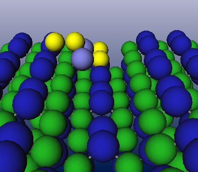
These structures are of sizes in the 10 nm range so that they cannot be prepared as free-standing objects but have to be embedded in matrices of similar material. Fortunately, a well known process can be used for this purpose which is the Stranski-Krastanow growth mode: If the thickness of an epitaxial film of a material with a slightly different lattice constant exceeds a certain value, the strain in the film is released by coalescence of the second and higher layer material into small three-dimensional islands of a layer density of about 1011 cm-2, i.e. containing some 104 atoms. The question of whether this "self-organization" is really Stranski-Krastonw growth or whether additional constraints are involved has been raised recently.
The semiconductor material of low dimensions is embedded into a matrix from the same lattice type but of larger band gap. This leads to a confinement of states at energies below the band edges of the embedding material. Since in most cases the lattice constants differ by some percent, the behavior of the confined carriers is influenced by elastic strain as well as piezoelectric polarization in polar media.
In the last decade a large number of different quantum wire (QW) and QD systems have been realized. Even first applications as, e.g., QD lasers have been developed. Nevertheless there is great demand for further investigations to achieve a detailed understanding of these systems. For these reasons we plan a discussion workshop which should cover two main topics in this field which are growth and characterization of semiconductor nanostructures as well as transport and optical properties.
Although in the final state one certainly has to rely on self-organizing processes, it is not clear at the moment whether a combination of stucturing from outside and self-organization have to be combined in order to prepare assembles of sharp enough size distribution. Also in order to study basic properties of localization, the preparation of low-dimensional structures on pre-structured surfaces showed great success. It is therefore a goal of the workshop to bring together scientist from three different areas: Experimentalists for the systematic study of the epitaxy and the different substrate surfaces, scientists whose concern is the characterization of the nanostructures with high resolution tools and also theoreticians who study the epitaxy on a microscopic basis . One topic to be discussed is the question of whether the QDs in the InAs/GaAs system are pure InAs or mixed InGaAs dots. Depending on preparation the composition seem to vary. In metallorganic gas phase epitaxy pure InAs dots have been observed (Dähne) whereas in migration-enhanced epitaxy and molecular beam epitaxy InGaAs dots have been observed (Bell, Shih).
The electronic and optical properties of these structures depend also on the preparation method. Optical measurements, e.g., photoluminescence measurements are mostly the first experimental tool to derive information about the structural quality of the grown samples. Therefore we plan as a further topic of the workshop to discuss about the electronic and optical properties. Due to the large number of data, even on spectroscopy from single QDs, there are specific questions raised for theory. We like to discuss the different methods to calculate single-particle quantum states in QDs with k.p.störungs theory (Stier) as well as with empirical pseudopotentials (Zunger). Furthermore, we would like also to enter the field of transport through nano-structures which will become more and more important in the future.
The "Tagungsstätte" Ringberg Castle supplies an excellent ambient and accommodation to bring together about 40 specialists in the above area for a fruitful and quite informal discussion.
On February 7, dinner will be served, and an evening session starts at 8 PM.
All oral contributions will be in the form of invited talks of 25 min., plus 5 min. discussion.
The workshop will end on February 10 before noon.
Preliminary schedule
| time | Wednesday, 7th | Thursday, 8th | Friday, 9th | Saturday, 10th |
| 9:00 AM | Epitaxy of III-V compounds | Excited States in QDs | Transport | |
| G. Bell | O. Stier | S. Goodnick | ||
| P. Kratzer | R. Heitz | R.J. Haug | ||
| K. Shiraishi | J. Finley | A. Wacker | ||
| 10:00 AM | Coffee | Coffee | Coffee | |
| Growth on the atomic scale | Single dot spectrocopy | QD-based devices / lasers | ||
| 11:00 AM | K. Jacobi | G. Abstreiter | D.G. Deppe | |
| G. Salamo | R. Warburton | P. Borri | ||
| J. Neugebauer | F. Henneberger | M. Grundmann | ||
| 12:30 PM | Lunch | Lunch | ||
| Posters | Excursion/Walk | |||
| Optical Properties of QDs | ||||
| 5:00 PM | Growth of Nanostructures | M. Bayer | ||
| 5:30 PM | T. Fukui | C. Lienau | ||
| V.M. Ustinov | A. Knorr | |||
| 6:30 PM | Dinner | Dinner | Candlelight Dinner | |
| Introductory talks | Characterisation of Qdots | |||
| 8:00 PM | G. Bauer | M. Dähne | ||
| C. Ratsch | K. Shih | |||
4. Information about Schloss Ringberg
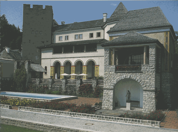
Schloss Ringberg
D-83700 Rottach-Egern
Germany
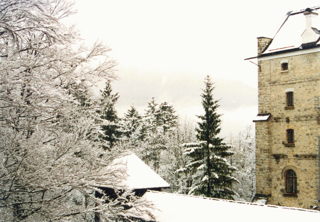
The weather in February is typically quite cold (average between -5 and 5
° C ) with occasional snowfall. Be prepared for winter-like weather.5. Submission of Abstracts
Please send the abstracts to the following address:
Registration Deadline: December 15, 2000
There will be no registration fee.
Board and lodging is offered as a package including the room rate for three nights, breakfast, lunch and dinner. Please note that credit cards are not accepted at Ringberg Castle. On Wednesday, February 7, there will be dinner only. On Saturday, February 10, breakfast will be served.To register, please send an e-mail with your name, affiliation and arrival time to:
The workshop will be sponsored by the Deutsche Forschungsgemeinschaft (DFG) and the Max-Plack-Gesellschaft (MPG).
![]()
This Page is maintained by: Peter Kratzer
Last update: February 1, 2001